
Guide to Circuit Board Assembly
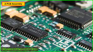
The circuit board assembly process combines the printed circuit boards (PCBs) with the electronic components to create a functional final product. The process involves using a soldering machine to connect the components to the conductive pathways engraved into the laminated copper sheets of the PCB. This makes the circuit board work as intended and enables it to perform the desired functions.
There are three primary types of circuit board assembly: Surface Mount Technology (SMT), Through-Hole Technology (THT) and mixed technology assembly. These differ in the type of soldering electronic components used, their assembly processes and the resulting characteristics of the finished circuit board. Before you begin the assembly process, consider the materials and components that will be utilized in your project.
This will help you decide on the best assembly method for your project. It is also important to consider the design needs of the various materials and components that are being used. This will ensure that they are optimally used and will not present any problems during the reflow soldering process.
A Step-By-Step Guide to Circuit Board Assembly
The first step in the circuit board assembly process is to apply solder paste to the pads of the circuit board. Then, the components are placed on the paste by a pick-and-place machine. This is followed by reflow soldering to make the electrical connections between the components and the PCB. Once the soldering is complete, the components and the traces are inspected to ensure that they are properly connected and have good contact.
To avoid signal issues and other problems that can occur during the circuit board assembly process, it is crucial to route your traces efficiently. This is especially true for power and signal traces. If possible, try to orient your tracks in a parallel fashion to reduce crosstalk and electromagnetic generation. If your tracks have to intersect with one another, make sure that they do so at right angles to minimize the capacitance and inductance between them.
In order to keep your circuit boards clean during the assembly process, you should use a masking process to protect the areas of the circuit board that are not being worked on. This will prevent the accidental insertion of foreign material and will also prevent the damage that occurs to the exposed surface during the soldering process.
Before you begin measuring your circuit boards, be sure that you have calculated the dimensions of each component. You can do this by using a measurement tool in your PCB software program. If your PCB has protrusions that extend past the edges of the outline box, it is important to note this during the measurement process so that your board can fit into the In-Plant Handler without causing any damage to your circuit boards. It is also important to be aware of the size limitations of your etching equipment.